From the MSPU story:
Microsoft’s researchers have created a curved camera sensor which they say solves one of the biggest issues with creating high-quality digital images.
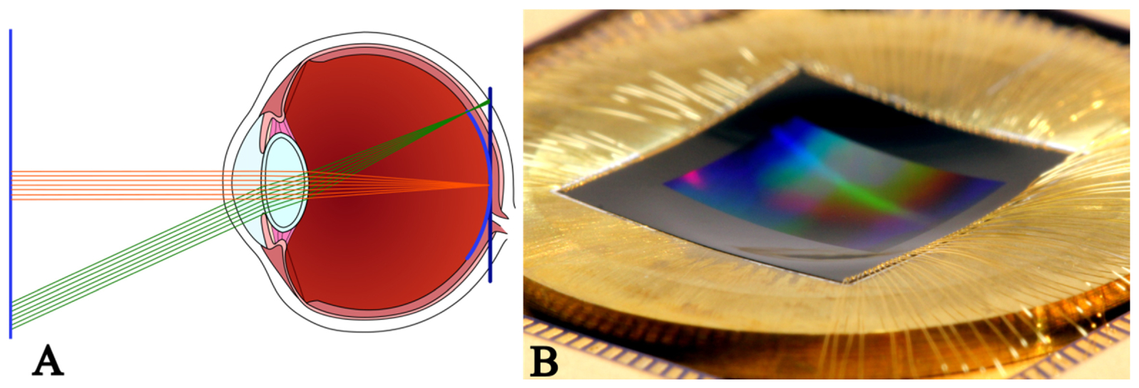
They note that lenses do not focus naturally on a flat surface like a camera sensor, but rather a curved spherical surface like the back of the eye.
This means that with flat sensors objects appear out of focus across the image. By curving the focal surface, Microsoft eliminates the need for the lens to address field curvature and can use the resulting optical design freedom to improve other aspects of the system. Specifically, the system can improve resolution, light-gathering capability, lateral chromatic aberration, distortion and illumination uniformity while also reducing system size, complexity and cost.
From the original paper:
The significant optical and size benefits of using a curved focal surface for imaging systems have been well studied yet never brought to market for lack of a high-quality, mass-producible, curved image sensor. In this work we demonstrate that commercial silicon CMOS image sensors can be thinned and formed into accurate, highly curved optical surfaces with undiminished functionality.
Our key development is a pneumatic forming process that avoids rigid mechanical constraints and suppresses wrinkling instabilities. A combination of forming-mold design, pressure membrane elastic properties, and controlled friction forces enables us to gradually contact the die at the corners and smoothly press the sensor into a spherical shape. Allowing the die to slide into the concave target shape enables a threefold increase in the spherical curvature over prior approaches having mechanical constraints that resist deformation, and create a high-stress, stretch-dominated state.
Our process creates a bridge between the high precision and low-cost but planar CMOS process, and ideal non-planar component shapes such as spherical imagers for improved optical systems. We demonstrate these curved sensors in prototype cameras with custom lenses, measuring exceptional resolution of 3220 line-widths per picture height at an aperture of f/1.2 and nearly 100% relative illumination across the field.
Though we use a 1/2.3” format image sensor in this report, we also show this process is generally compatible with many state of the art imaging sensor formats. By example, we report photogrammetry test data for an APS-C sized silicon die formed to a 30° subtended spherical angle. These gains in sharpness and relative illumination enable a new generation of ultra-high performance, manufacturable, digital imaging systems for scientific, industrial, and artistic use.
So, essentially, multi-element optics (e.g. Lumia 1020 artistic interpretation below) that have traditionally been optimised to correct for such aberrations can now (in the future) be drastically simplified, allowing for sharper, better photos, with almost no size penalty, probably a weight saving, and the likelihood that OIS will be cheaper and more effective too.